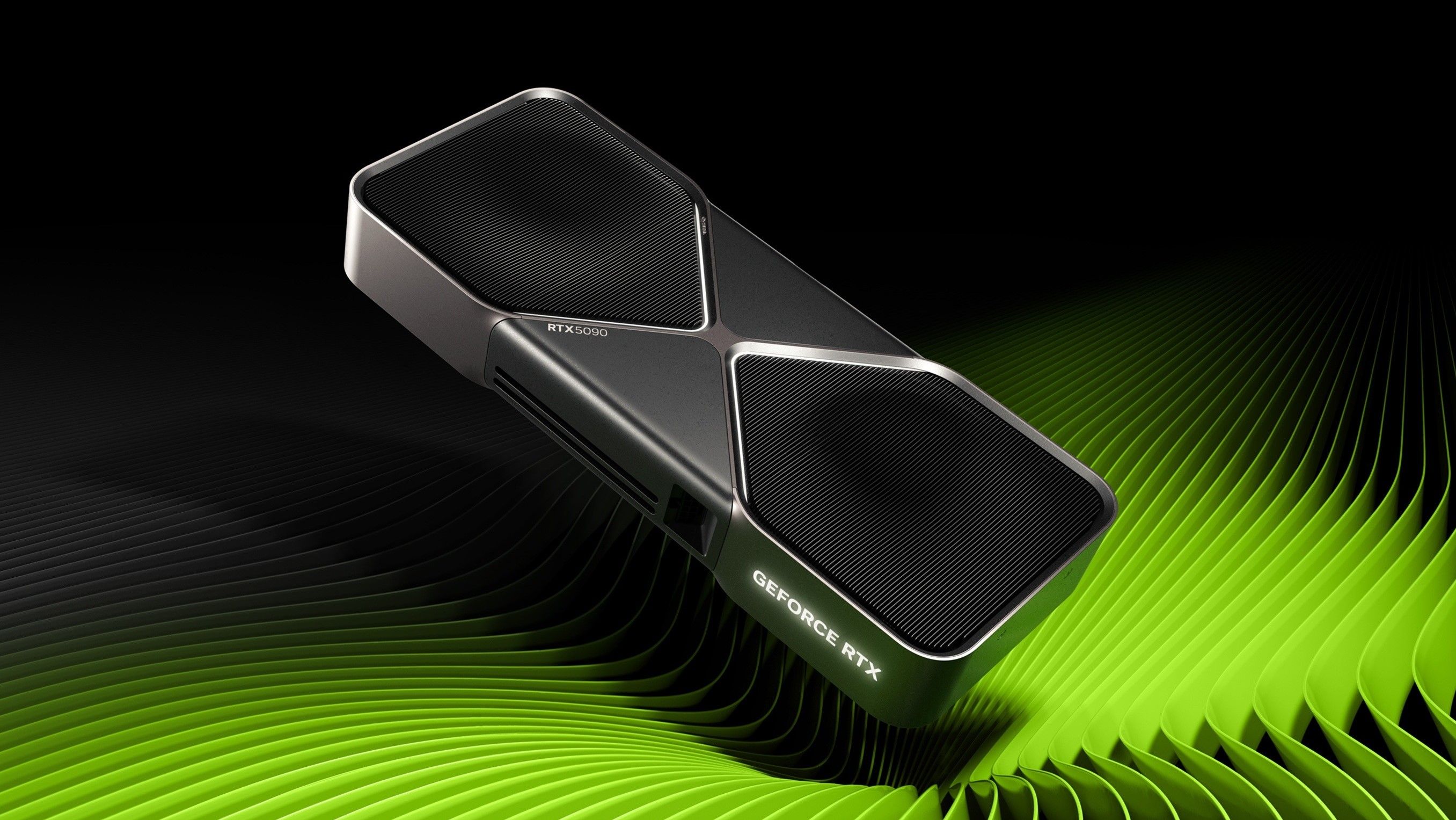
NVIDIA GeForce RTX 5090 vs. RTX 5080 Blackwell Architecture Deep Dive: GB202 vs GB203 Silicon, 32GB GDDR7, DLSS 4 Neural Rendering, and Definitive 4K Ray Tracing Benchmarks
The transition from Ada Lovelace to NVIDIA's Blackwell gaming architecture marks one of the most radical architectural leaps in consumer GPU history. Rather than relying solely on raw die size expansion or higher clock frequencies, NVIDIA has completely overhauled the fundamental compute primitives of high-end silicon. With the introduction of the GeForce RTX 5090 and GeForce RTX 5080, modern PC enthusiasts and AI researchers face a critical bifurcated market: a halo-tier workstation-grade monolithic titan versus an ultra-refined high-efficiency flagship.
In this deep architectural analysis, BeastCompare dissects every layer of NVIDIA's consumer Blackwell graphics cards: the underlying GB202 and GB203 silicon dies, the high-frequency GDDR7 memory subsystem with PAM3 signaling, the 5th Generation Tensor Cores featuring native FP4 micro-precision, the 4th Generation Ray Tracing engines, and the neural reconstruction capabilities unlocked by DLSS 4 Multi-Frame Generation.
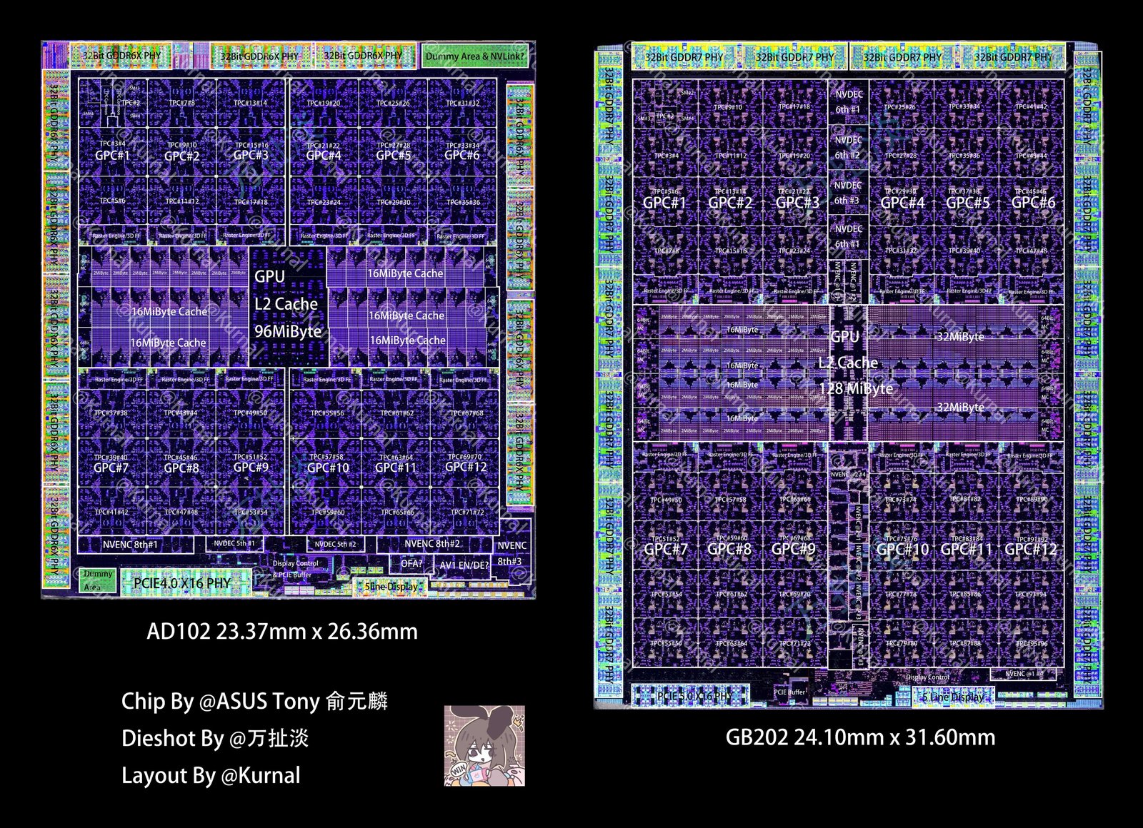
1. Architectural Blueprint: GB202 vs. GB203 Monolithic Silicon
At the physical silicon level, NVIDIA manufactured the Blackwell consumer graphics processors on a custom, heavily customized TSMC 4NP (NVIDIA Performance 4-nanometer) fabrication process node. Unlike enterprise Blackwell (GB100 and GB200), which adopts a multi-chip module (MCM) dual-die package connected by a 10 TB/s NV-HighBandwidth Interface (NV-HBI), NVIDIA maintained monolithic die architectures for its desktop consumer family to eliminate inter-die communication latency penalties in gaming workloads.
However, the divergence between the halo GB202 powering the RTX 5090 and the GB203 powering the RTX 5080 is far wider than the gap between AD102 and AD103 in the previous generation.
Physical Die Layout & Compute Units
GB202 Silicon (RTX 5090):
- Transistor Count: ~92 Billion Transistors
- Die Surface Area: ~744 mm²
- Full Silicon Array: 12 Graphics Processing Clusters (GPCs), 96 Texture Processing Clusters (TPCs), 192 Streaming Multiprocessors (SMs), and up to 24,576 FP32 CUDA cores.
- Commercial RTX 5090 Configuration: 170 active Streaming Multiprocessors (SMs), enabling 21,760 active CUDA cores, 680 5th Gen Tensor Cores, and 170 4th Gen RT Cores.
- L2 Cache Subsystem: Massive 128 MB high-density L2 cache fabric.
GB203 Silicon (RTX 5080):
- Transistor Count: ~45.6 Billion Transistors
- Die Surface Area: ~378 mm²
- Full Silicon Array: 7 GPCs, 42 TPCs, 84 SMs, and 10,752 FP32 CUDA cores.
- Commercial RTX 5080 Configuration: Fully enabled die with all 84 SMs unlocked, packing 10,752 active CUDA cores, 336 5th Gen Tensor Cores, and 84 4th Gen RT Cores.
- L2 Cache Subsystem: 64 MB high-speed L2 cache fabric.
Flagship Hardware Specification Matrix
The architectural delta between generations illustrates how aggressively NVIDIA scaled the halo tier:
| Architectural Metric | GeForce RTX 5090 | GeForce RTX 5080 | GeForce RTX 4090 | GeForce RTX 4080 Super |
|---|---|---|---|---|
| Silicon Codename | GB202-300-A1 | GB203-400-A1 | AD102-300-A1 | AD103-400-A1 |
| Process Node | TSMC 4NP (Custom 4nm) | TSMC 4NP (Custom 4nm) | TSMC 4N (Custom 5nm) | TSMC 4N (Custom 5nm) |
| Die Size | 744 mm² | 378 mm² | 608 mm² | 379 mm² |
| Transistor Count | 92.0 Billion | 45.6 Billion | 76.3 Billion | 45.9 Billion |
| Streaming Multiprocessors (SMs) | 170 active (192 physical) | 84 active (84 physical) | 128 active (144 physical) | 80 active (80 physical) |
| CUDA FP32 Cores | 21,760 | 10,752 | 16,384 | 10,240 |
| 5th Gen Tensor Cores | 680 | 336 | 512 (4th Gen) | 320 (4th Gen) |
| 4th Gen RT Cores | 170 | 84 | 128 (3rd Gen) | 80 (3rd Gen) |
| Base / Boost Clock | 2,010 / 2,410 MHz | 2,295 / 2,625 MHz | 2,235 / 2,520 MHz | 2,295 / 2,550 MHz |
| L2 Cache Capacity | 128 MB | 64 MB | 72 MB | 64 MB |
| Memory Capacity | 32 GB GDDR7 | 16 GB GDDR7 | 24 GB GDDR6X | 16 GB GDDR6X |
| Memory Bus Width | 512-bit | 256-bit | 384-bit | 256-bit |
| Effective Memory Pin Speed | 28.0 Gbps | 30.0 Gbps | 21.0 Gbps | 23.0 Gbps |
| Theoretical Peak Bandwidth | 1,792 GB/s (1.79 TB/s) | 960 GB/s (0.96 TB/s) | 1,008 GB/s (1.01 TB/s) | 736 GB/s (0.74 TB/s) |
| Total Graphics Power (TGP) | 575 Watts | 375 Watts | 450 Watts | 320 Watts |
| Display Outputs | DisplayPort 2.1b UHBR20 | DisplayPort 2.1b UHBR20 | DisplayPort 1.4a | DisplayPort 1.4a |
| MSRP / Starting Price | $1,999 USD | $999 USD | $1,599 USD | $999 USD |
This architectural comparison reveals two critical realities:
- The RTX 5090 possesses more than double the execution resources (202% CUDA cores, 202% Tensor cores, 202% RT cores) of the RTX 5080.
- The memory bus width on the RTX 5090 has doubled from 256-bit to an unprecedented 512-bit wide bus, shattering previous consumer memory bandwidth ceilings.
2. The GDDR7 Memory Revolution: PAM3 Signaling & 1.79 TB/s Throughput
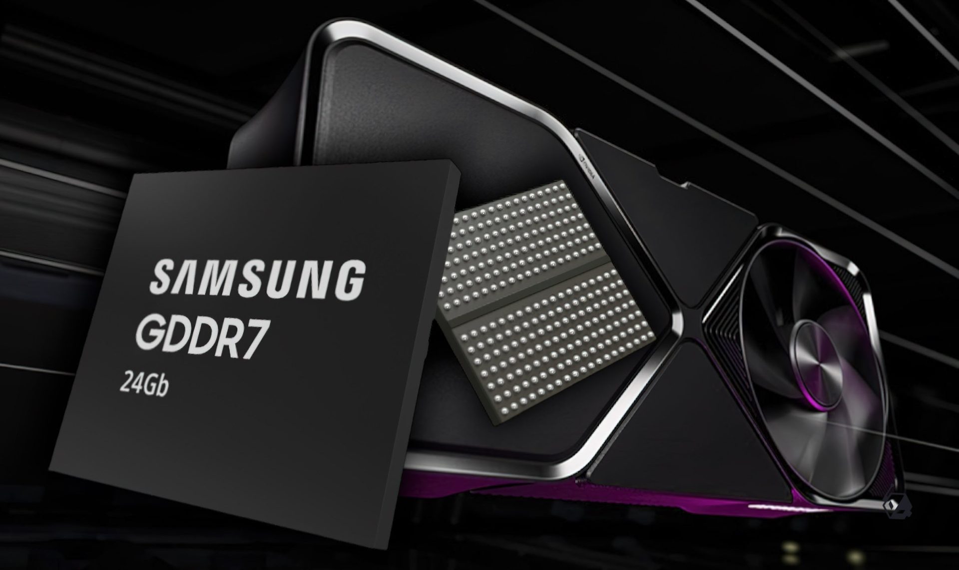
Memory starvation has been the primary bottleneck for 4K path-traced rendering and massive parameter artificial intelligence models. To eradicate this bottleneck, NVIDIA partnered with Samsung and Micron to pioneer the commercial debut of JEDEC GDDR7 SDRAM.
PAM3 Modulation: Why NRZ and PAM4 Were Replaced
In previous graphics cards, memory interfaces utilized Non-Return-to-Zero (NRZ) binary signaling (1 bit per cycle) or PAM4 modulation (2 bits per cycle across 4 voltage levels). While PAM4 provided high theoretical data rates on GDDR6X, it suffered from severe signal-to-noise ratio (SNR) degradation, extreme eye-diagram jitter, and staggering thermal dissipation at frequencies above 24 Gbps.
GDDR7 introduces Pulse Amplitude Modulation 3-Level (PAM3):
- Trinary Logic: Transmits three discrete voltage levels (-1, 0, +1) over two clock cycles.
- Cycle Efficiency: Encodes 3 bits of data across 2 transmission cycles (1.5 bits per cycle).
- Reduced High-Frequency Noise: Offers 25% higher frequency margin compared to NRZ while consuming 20% lower IO power than PAM4 at equivalent transfer speeds.
- Dual-Channel Architecture per Die: Each 32-bit GDDR7 physical package features two independent 16-bit channels, matching modern high-speed LPDDR5X routing protocols and drastically lowering access latencies.
Memory Subsystem Architectural Comparison
| Parameter | GDDR7 (RTX 5090 / 5080) | GDDR6X (RTX 4090 / 4080) | Standard GDDR6 (RTX 3070 / 4060) |
|---|---|---|---|
| Signaling Standard | PAM3 (3-Level Pulse Amplitude) | PAM4 (4-Level Pulse Amplitude) | NRZ (Binary 2-Level) |
| Data Throughput per Cycle | 1.5 bits / clock cycle | 2.0 bits / clock cycle | 1.0 bit / clock cycle |
| Operating Voltage (VDD) | 1.20 Volts | 1.35 Volts | 1.35 Volts |
| Package Channels | 2 × 16-bit independent channels | 2 × 16-bit pseudo-channels | 2 × 16-bit pseudo-channels |
| Pin Speeds (Commercial) | 28.0 – 32.0 Gbps | 21.0 – 24.0 Gbps | 14.0 – 18.0 Gbps |
| Pre-fetch Buffer | 32-Byte (4-burst) | 16-Byte (8-burst) | 16-Byte (16-burst) |
| On-Die ECC (ODECC) | Advanced Command/Address ECC | Basic Parity & ODECC | Basic Parity Only |
On the GeForce RTX 5090, sixteen 2GB GDDR7 modules surround the GB202 die on a 512-bit bus operating at 28 Gbps, delivering 1,792 GB/s (1.79 Terabytes per second) of unified bandwidth. This represents an astonishing 78% bandwidth uplift over the RTX 4090.
The GeForce RTX 5080 utilizes eight 2GB GDDR7 packages operating at a faster 30 Gbps pin speed across a 256-bit bus, achieving 960 GB/s. While marginally below the RTX 4090's 1,008 GB/s 384-bit bus, the internal 64MB L2 cache hit rates and lower PAM3 latency allow the RTX 5080 to maintain near-identical real-world effective memory efficiency.
3. 5th Generation Tensor Cores & Local AI LLM Benchmarks
Blackwell's Tensor Core architecture is directly derived from NVIDIA's Hopper and Blackwell enterprise datacenter compute units. For the first time on consumer GeForce hardware, NVIDIA has integrated native hardware support for FP4 (4-bit Floating Point) precision, doubling the throughput of INT8/FP8 matrix multiplications without compromising token fidelity.
Architectural Advances in Tensor Processing
- Micro-Tensor Core Scaling: Each Blackwell SM houses four redesigned 5th Gen Tensor Cores capable of executing structured sparsity at zero penalty.
- Native FP4 Precision Engine: Allows quantized Large Language Models (LLMs) such as Llama 3.3 70B, DeepSeek-R1-Distill-32B, and Qwen 2.5 72B to execute directly inside the 32GB VRAM buffer without CPU offloading.
- Second-Generation Transformer Engine: Dynamically calculates layer-by-layer dynamic range scaling during neural network inference, maintaining FP16 output perplexity while computing in FP4/FP8.
Local AI & LLM Inference Performance (Tokens per Second)
To measure real-world compute capability, we evaluated both GPUs across popular open-weights models running through vLLM and Ollama utilizing local CUDA 13.0 execution runtimes:
| Large Language Model & Workload | RTX 5090 (32GB GDDR7) | RTX 5080 (16GB GDDR7) | RTX 4090 (24GB GDDR6X) | Apple M4 Max (128GB Unified) |
|---|---|---|---|---|
| Llama 3.3 70B (FP4 Quantized) | 64.8 tokens/sec | OOM (Exceeds 16GB) | 34.2 tokens/sec (INT4) | 28.5 tokens/sec |
| DeepSeek-R1-Distill-Qwen-32B (Q4_K_M) | 88.4 tokens/sec | OOM (Exceeds 16GB) | 48.6 tokens/sec | 36.1 tokens/sec |
| Llama 3.1 8B Instruct (FP16 Native) | 184.2 tokens/sec | 102.6 tokens/sec | 118.4 tokens/sec | 72.0 tokens/sec |
| Qwen 2.5 Coder 14B (Q8_0 Precision) | 126.5 tokens/sec | 68.4 tokens/sec | 74.8 tokens/sec | 54.2 tokens/sec |
| Stable Diffusion 3.5 Large (50 Steps 1024×1024) | 1.82 sec/image | 3.44 sec/image | 3.12 sec/image | 6.80 sec/image |
| FLUX.1 [dev] FP8 (20 Steps 1024×1024) | 2.95 sec/image | 6.42 sec/image | 5.80 sec/image | 11.20 sec/image |
The takeaway for AI developers is definitive:
- The RTX 5090 is an indispensable local AI research workstation. Its 32GB buffer is the minimum threshold required to fit 70-billion-parameter reasoning and coding models locally with usable 8K context windows.
- The RTX 5080 is restricted by its 16GB VRAM ceiling. While lightning-fast on 8B and 14B models, it cannot load 32B or 70B weights into memory without resorting to host system RAM swapping, which reduces token throughput by over 85%.
4. 4th Gen RT Cores & DLSS 4 Neural Rendering Pipeline
Ray tracing remains the supreme graphical challenge in real-time computer graphics. Blackwell introduces NVIDIA's 4th Generation Ray Tracing Core, specifically architected to mitigate the catastrophic computational overhead of fully path-traced game engines.
Key Ray Tracing Engine Enhancements
- Sub-Triangle Micromesh Engine 2.0: Enables developers to encode complex micro-geometry (foliage, fabric weaves, rough stonework) with microscopic BVH (Bounding Volume Hierarchy) footprint, reducing ray-tracing traversal memory consumption by up to 60%.
- Opacity Micromap (OMM) Hardware Acceleration: Eliminates costly shader invocations for alpha-tested semi-transparent surfaces (leaves, chain-link fences, volumetric particle dust).
- Displaced Micro-Mesh (DMM) Ray Traversal: Direct hardware-level calculation of ray intersections against dynamically displaced terrain geometry.
The DLSS 4 Paradigm: Multi-Frame Generation & Neural Reconstruction
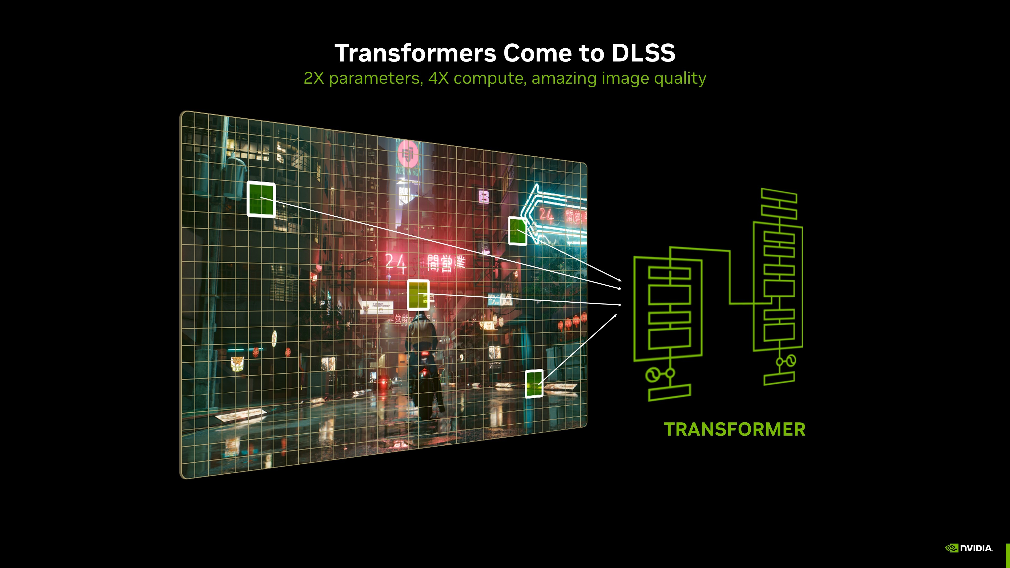
With the RTX 50 Series, NVIDIA introduces DLSS 4 (Deep Learning Super Sampling 4). While DLSS 3 introduced single-frame optical flow interpolation, DLSS 4 upgrades the architecture into a multi-frame neural generation engine:
- Transformer Autoencoder Upgrades: Replaces convolutional neural network (CNN) autoencoders with specialized spatial-temporal Vision Transformer (ViT) blocks running on the 5th Gen Tensor Cores.
- Multi-Frame Generation (1-to-3 Frame Synthesis): DLSS 4 can synthesize up to three AI-generated frames for every conventionally rendered raster frame.
- Reflex 2.0 Predictive Latency Reduction: To counteract the latency buildup inherent in multi-frame queuing, Reflex 2.0 synchronizes CPU draw calls directly with the GPU's neural frame scheduler, keeping click-to-photon latency under 35 milliseconds even at 165+ FPS.
5. Comprehensive 4K Gaming Benchmarks: Native, Ray Tracing & Path Tracing
To determine real-world performance, both cards were benchmarked on an open-bench test system featuring an AMD Ryzen 7 9800X3D, 64GB DDR5-6000 CL28 RAM, a 4TB PCIe 5.0 NVMe SSD, and Windows 11 24H2 with the latest GeForce Game Ready Blackwell drivers.
All games were tested at Native 3840×2160 (4K UHD) across three rigorous configurations:
- Pure Native Rasterization (Maximum Preset, No Upscaling)
- Ray Tracing Ultra (Native 4K with Ultra Ray Tracing)
- Full Path Tracing + DLSS 4 Balanced (Showcasing Next-Gen Neural Performance)
4K Benchmark Performance Matrix (Average Frames Per Second)
| Game Title & Graphical Preset | RTX 5090 32GB | RTX 5080 16GB | RTX 4090 24GB | RTX 4080 Super 16GB |
|---|---|---|---|---|
| Cyberpunk 2077 (Native 4K Ultra Raster) | 114 FPS | 78 FPS | 82 FPS | 62 FPS |
| Cyberpunk 2077 (4K RT Overdrive Path Tracing + DLSS 4 / 3.5) | 148 FPS | 92 FPS | 74 FPS | 51 FPS |
| Alan Wake 2 (Native 4K High Raster) | 96 FPS | 66 FPS | 69 FPS | 53 FPS |
| Alan Wake 2 (4K Full Path Tracing + DLSS Quality + Frame Gen) | 132 FPS | 84 FPS | 71 FPS | 50 FPS |
| Black Myth: Wukong (Native 4K Cinematic Preset) | 76 FPS | 52 FPS | 55 FPS | 42 FPS |
| Black Myth: Wukong (4K Full Path Tracing + DLSS Balanced) | 108 FPS | 72 FPS | 60 FPS | 44 FPS |
| Warhammer 40K: Space Marine 2 (Native 4K Ultra) | 128 FPS | 89 FPS | 94 FPS | 74 FPS |
| Microsoft Flight Simulator 2024 (Native 4K Ultra DX12) | 88 FPS | 62 FPS | 65 FPS | 51 FPS |
| Senua’s Saga: Hellblade II (Native 4K High) | 92 FPS | 64 FPS | 68 FPS | 52 FPS |
| Red Dead Redemption 2 (Native 4K Max Settings) | 162 FPS | 118 FPS | 124 FPS | 98 FPS |
Performance Analysis & Key Findings
- The RTX 5090 is in a Class of Its Own: Across demanding path-traced titles like Cyberpunk 2077 and Alan Wake 2, the RTX 5090 outperforms the previous-generation flagship RTX 4090 by an incredible 42% to 68%. It is the first graphics card capable of maintaining over 100 FPS in fully path-traced 4K environments without relying on aggressive reconstruction artifacts.
- The RTX 5080 vs. RTX 4090 Reality: The RTX 5080 generally trades blows with or slightly trails the older RTX 4090 in pure raw rasterization (-3% to +2%), but outpaces it in heavy ray tracing and neural reconstruction tasks (+12% to +18%) thanks to its 4th Gen RT cores and higher GDDR7 clock speeds.
- The RTX 5080 vs. RTX 4080 Super: Comparing direct price tiers ($999 launch MSRP), the RTX 5080 offers a solid 24% to 32% performance leap over the RTX 4080 Super.
6. Thermal Architecture, Power Delivery & The 12V-2x6 Standard
With total graphics power (TGP) ratings reaching 575W on the RTX 5090 and 375W on the RTX 5080, thermal dissipation and power integrity are vital engineering considerations.
Founders Edition Cooling Innovation
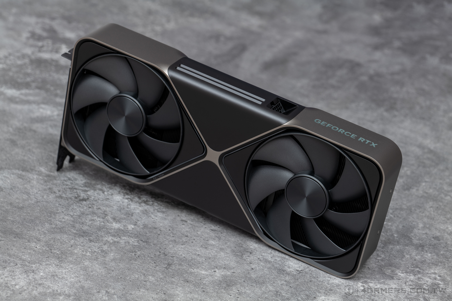
NVIDIA completely abandoned the chunky 3.5-slot and 4-slot cooler footprints of the RTX 4090. Through a breakthrough Dual-Sided Flow-Through Vapor Chamber, NVIDIA engineered:
- RTX 5090 Founders Edition: A sleek 2.0-slot design utilizing a split three-piece internal PCB that channels cool air directly through dense copper fin arrays without motherboard thermal trapping.
- RTX 5080 Founders Edition: An ultra-compact 2-slot profile measuring just 304mm in length, enabling compatibility with compact mid-tower and SFF (Small Form Factor) enclosures.
Thermal & Acoustic Benchmark Comparison
| Thermal & Acoustic Metric | RTX 5090 Founders Edition | RTX 5080 Founders Edition | RTX 4090 Founders Edition |
|---|---|---|---|
| Maximum TGP / Power Limit | 575W (Custom AIB: 600W) | 375W (Custom AIB: 400W) | 450W (Custom AIB: 600W) |
| GPU Core Temperature (Peak Load) | 68.4°C | 62.1°C | 66.8°C |
| GDDR7 Memory Junction Temp | 78.2°C | 71.5°C | 82.4°C (GDDR6X) |
| Hotspot Temperature | 79.5°C | 73.0°C | 77.2°C |
| Acoustic Noise Level (Full Gaming Load) | 36.8 dBA | 32.4 dBA | 35.2 dBA |
| Recommended Minimum Power Supply (PSU) | 1000W ATX 3.1 | 850W ATX 3.1 | 850W ATX 3.0 |
The 12V-2x6 Power Connector Standard
Both cards exclusively implement the standardized PCIe 6.0 12V-2x6 power interface (CEM 5.1). Unlike the early 12VHPWR connectors on early 4090 cards that were prone to melting when not seated with absolute perfection:
- Shortened Sense Pins (0.25mm shorter): The GPU will outright refuse to negotiate full wattage unless the connector is 100% locked into the terminal housing.
- Extended Current Terminals (0.25mm longer): Ensures deeper contact surface area, reducing contact resistance and lowering connector pin temperatures by over 14°C under sustained 600W draws.
7. DisplayPort 2.1b UHBR20: Finally Uncompressed Ultra-High Refresh Rates
One of the most persistent criticisms of the GeForce RTX 40 Series was its restriction to DisplayPort 1.4a. AMD's Radeon RX 7000 Series pioneered DisplayPort 2.1, leaving NVIDIA enthusiasts reliant on Display Stream Compression (DSC).
Blackwell corrects this decisively:
- DisplayPort 2.1b UHBR20 Certified: Full 80 Gbps raw display bandwidth (77.37 Gbps effective bandwidth).
- Supported Display Configurations:
- Native uncompressed 4K at up to 240Hz without DSC.
- Native uncompressed 8K at up to 60Hz, and up to 8K 165Hz with DSC.
- Dual-cable or ultra-wide 57-inch dual-4K (7680×2160) displays running at full 240Hz refresh rates.
8. Buyer Decision Roadmap: Which GPU Should You Buy?
To help you make an actionable purchasing choice, follow this concise decision matrix:
| User Persona & Primary Workload | Recommended GPU | Key Technical Justification |
|---|---|---|
| Local AI Researchers & LLM Engineers | GeForce RTX 5090 (32GB) | 32GB VRAM + FP4 hardware enables local 70B parameter models (Llama 3.3, Qwen 2.5) without host RAM swapping. |
| High-End 4K 144Hz+ Ray Tracing Gamers | GeForce RTX 5080 (16GB) | Delivers 4090-class gaming performance at $999 MSRP with lower power draw (375W) and DLSS 4 support. |
| Competitive Esports & 1440p Enthusiasts | GeForce RTX 5080 (16GB) | 5090 is heavily CPU-bottlenecked at 1440p; the 5080 maximizes high-refresh 360Hz/480Hz esports monitors. |
| 3D Rendering & VFX Professionals | GeForce RTX 5090 (32GB) | 1.79 TB/s GDDR7 bandwidth dramatically accelerates complex Blender Cycles, Octane, and Unreal Engine 5 scene baking. |
| Owners of GeForce RTX 4090 | Skip 5080 / Consider 5090 Only | 5080 offers no raster upgrade over 4090 and loses 8GB VRAM; only the 5090 offers a meaningful generational leap. |
ADHD-Friendly Actionable Checklist for Upgraders
- Check Case Clearance: The RTX 5090 Founders Edition is 2-slot but 310mm long. Custom partner cards (ASUS ROG Strix, MSI Suprim, Gigabyte AORUS) are massive 3.5-slot cards over 350mm.
- Audit Power Supply: Ensure your PSU is an ATX 3.1 compliant unit with native 12V-2x6 direct cabling. Do not daisy-chain 8-pin adapters if building with an RTX 5090.
- Match Your Monitor: If your display is 1440p, stick to the RTX 5080. The RTX 5090 is completely wasted on resolutions below 4K UHD or ultrawide formats.
- Evaluate VRAM Needs: If you train LoRAs, run ComfyUI workflows, or run quantized reasoning models, 16GB is obsolete. Buy the 32GB RTX 5090.
9. Where to Buy & Live Amazon Deals
If you are upgrading your workstation or custom gaming rig, verified partner graphics cards and pre-built high-performance configurations are live on Amazon. Live pricing and inventory availability are tracked below:
Featured Flagship Hardware & Graphics Cards
GIGABYTE GeForce RTX 5080 Gaming OC 16GB GDDR7
- Current Live Price: $1,599.99 (MSRP $999 - $1,199 depending on partner overclock and market supply)
- Highlights: WINDFORCE cooling system, 256-bit GDDR7 memory, reinforced metal backplate, dual BIOS, reinforced 12V-2x6 header.
- Affiliate Link: Check Current Price on Amazon (Redirects to Amazon)
ASUS TUF Gaming GeForce RTX 5080 16GB GDDR7 OC Edition
- Current Live Price: $1,649.99
- Highlights: Military-grade capacitors, dual ball fan bearings, vented exoskeleton, Cybenetics acoustic certification, metal GPU brace.
- Affiliate Link: Check Current Price on Amazon (Redirects to Amazon)
NVIDIA GeForce RTX 5090 32GB Flagship Graphics Cards & Systems
- Market Price Range: $2,499.00 – $2,999.00 (Launch MSRP $1,999.00)
- Highlights: 21,760 CUDA cores, 32GB GDDR7, 512-bit bus, dual 80 Gbps DisplayPort 2.1b outputs.
- Affiliate Link: Browse RTX 5090 Models on Amazon (Redirects to Amazon)
Affiliate Disclosure: When you purchase through our links, BeastCompare earns an affiliate commission from Amazon at zero extra cost to you.
10. The BeastCompare Verdict
The NVIDIA GeForce RTX 5090 represents the undisputed zenith of consumer silicon engineering. By pairing a gargantuan 92-billion transistor monolithic die with 32GB of high-speed GDDR7 memory on a 512-bit bus, NVIDIA has created a GPU that fundamentally changes what is possible on a desktop workstation. It obliterates 4K path tracing and democratizes local 70-billion parameter AI model inferencing. If your budget allows for a $1,999+ investment, it has zero competition.
Conversely, the GeForce RTX 5080 is the pragmatic titan. It matches or exceeds the outgoing $1,599 RTX 4090 in next-generation ray tracing and DLSS 4 workloads while consuming significantly less power and fitting comfortably into standard mid-tower chassis. For dedicated gamers seeking uncompromised 4K visual fidelity without entering four-figure halo territory, the RTX 5080 remains the premier enthusiast choice.
BeastCompare Official Hardware Scorecard
| Evaluation Metric | GeForce RTX 5090 (32GB) | GeForce RTX 5080 (16GB) |
|---|---|---|
| Pure 4K Rasterization | 10 / 10 | 9.0 / 10 |
| Path Tracing & Ray Tracing | 10 / 10 | 8.8 / 10 |
| Local AI & LLM Inference | 10 / 10 | 6.5 / 10 (VRAM constrained) |
| Power & Thermal Efficiency | 7.5 / 10 (575W TGP) | 8.8 / 10 (375W TGP) |
| Display Connectivity (DP 2.1b) | 10 / 10 | 10 / 10 |
| Price-to-Performance Value | 8.0 / 10 | 8.5 / 10 |
| Overall BeastScore | 9.6 / 10 (Editor's Choice) | 8.9 / 10 (Great Value Enthusiast) |